Large AI models are driving steadily higher demand for GPUs, HBM high bandwidth memory, and high speed data exchange, making advanced semiconductor manufacturing increasingly important. Traditional chip manufacturing systems struggle to meet AI chips’ requirements for power consumption, bandwidth, and transistor density at the same time.
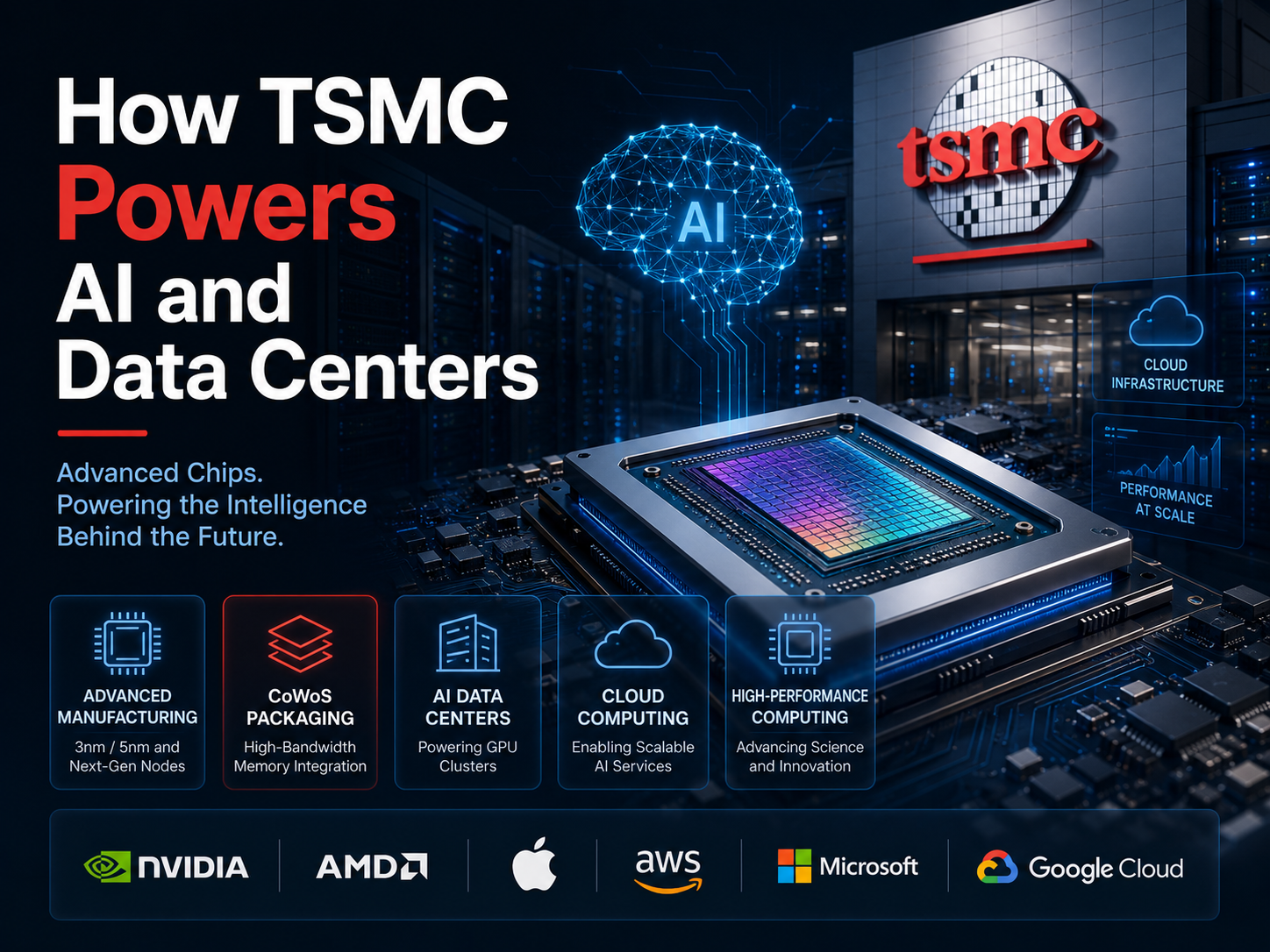
TSM applications in AI and data centers now cover AI GPU manufacturing, advanced packaging, cloud computing servers, high performance computing, and AI data center supply chains. Advanced wafer manufacturing capability has also gradually become an important part of global competition in AI infrastructure.
What Is TSM’s Role in the AI Chip Market
TSM’s core role in the AI chip market is serving as an important manufacturing platform for global AI GPUs and high performance AI chips. NVIDIA, AMD, and many cloud computing companies all rely on TSMC’s advanced processes to produce AI chips.
The performance of AI GPUs fundamentally depends on transistor density, power control, and high speed data exchange. TSMC’s 5nm and 3nm processes help AI chip companies integrate more computing units into a smaller area.
From an industry structure perspective, TSMC is closer to the underlying manufacturing platform within the AI chip ecosystem. AI chip companies are responsible for GPU architecture design, while TSMC turns those GPU designs into chips that can be mass produced.
Growth in AI chip demand has further strengthened TSMC’s position in the global semiconductor industry. The larger GPU order volumes become, the more obvious the dependence on advanced wafer manufacturing resources tends to be.
Compared with traditional consumer electronics chips, AI GPUs require greater stability from advanced process technologies. As a result, large AI companies usually secure advanced process capacity over the long term.
How TSM Supports AI Data Center GPU Manufacturing
AI data center GPU manufacturing fundamentally depends on advanced wafer manufacturing and high density packaging systems. During AI model training, large numbers of GPUs must continuously perform high speed parallel computing.
TSMC uses advanced processes to manufacture the core wafers for AI GPUs. The higher the transistor density, the stronger the AI computing capability and the lower the energy consumption a GPU can usually deliver.
CoWoS packaging handles the high speed connection between GPUs and HBM high bandwidth memory. AI model training frequently calls on video memory data, so the efficiency of data exchange between GPUs and memory is extremely important.
Below is the main collaboration structure in AI GPU manufacturing:
| Module |
Core Function |
TSM Involvement |
| GPU architecture |
AI computing |
Wafer manufacturing |
| HBM memory |
Data caching |
Packaging integration |
| CoWoS packaging |
High speed interconnection |
Advanced packaging |
| AI servers |
Model training |
Chip supply |
This manufacturing system means TSMC is not only responsible for wafer production, but also deeply involved in AI GPU performance optimization and packaging coordination.
Why AI Model Training Depends on TSM’s Advanced Processes
AI model training depends on advanced processes mainly because of the need for computing density and energy efficiency. Large language models usually require extremely large GPU clusters, so power control in AI chips is critical.
Advanced processes make it possible to integrate more transistors into a smaller area. The more GPU computing units there are, the stronger AI model training efficiency usually becomes.
AI data centers also need to control energy consumption. TSMC’s advanced processes can reduce GPU power consumption, helping improve the overall energy efficiency of AI data centers.
From a technical perspective, advanced transistor structures can also improve GPU frequency and data throughput. The larger the parameter scale of an AI model becomes, the higher the requirements tend to be for GPU computing efficiency.
This trend means competition in AI computing power is no longer only about software. It is also a competition in advanced manufacturing capability. Advanced processes have gradually become an important part of AI infrastructure.
What Are the Use Cases for TSM CoWoS Advanced Packaging
TSM CoWoS packaging is mainly used in AI GPUs, high performance computing, and cloud computing servers. CoWoS technology can improve data transfer efficiency between GPUs and HBM memory.
Traditional packaging methods struggle to meet the high bandwidth demands of AI GPUs. During AI model training, large numbers of parameters are constantly exchanged between GPUs and video memory, so packaging structure directly affects training efficiency.
CoWoS packaging can integrate GPUs and multiple sets of HBM memory into a single package structure. The high speed interconnect system can reduce data latency and improve AI data throughput.
CoWoS is currently mainly used in:
-
AI GPUs
-
AI data centers
-
HPC supercomputing
-
Cloud computing servers
The importance of CoWoS lies not only in performance improvement, but also in helping reduce system power consumption. When AI data centers deploy large numbers of GPUs, packaging efficiency directly affects heat dissipation and energy management.
As AI GPU shipments continue to expand, CoWoS has also become a key resource in the global semiconductor supply chain.
How TSM Affects Cloud Computing and AI Infrastructure
TSM’s impact on the cloud computing industry comes fundamentally from its ability to supply AI GPUs and server chips. AWS, Microsoft Azure, and Google Cloud all need large numbers of AI GPUs to support model training and inference services.
The pace of cloud computing platform expansion directly affects demand for advanced processes. The larger AI services become, the greater the demand usually is for GPU and advanced packaging resources.
From an infrastructure perspective, AI cloud platforms have gradually come to depend on coordination between GPU clusters and high speed networks. TSMC’s advanced process and packaging systems have therefore become an important part of the cloud computing supply chain.
GPUs, CPUs, and networking chips in AI data centers rely heavily on TSMC manufacturing. Advanced wafer manufacturing capability has gradually begun to affect the deployment efficiency of global AI cloud services.
Unlike traditional internet servers, AI data centers have higher requirements for chip performance and energy efficiency, so the importance of advanced semiconductor manufacturing continues to rise.
TSM’s applications in high performance computing now cover AI supercomputing, scientific computing, and enterprise level HPC systems. High performance computing usually requires GPU clusters, low latency networks, and high speed data synchronization.
Supercomputers and AI supercomputing platforms usually use large numbers of GPUs and high performance CPUs. TSMC’s advanced processes can support higher computing density in HPC chips.
High performance computing tasks usually include:
-
AI model training
-
Climate simulation
-
Drug development
-
Financial computing
GPUs and CPUs in HPC systems need to continuously exchange data at high speed, making advanced packaging and low power design very important.
Structurally, AI supercomputing has gradually become an important part of the HPC system. The boundary between AI and high performance computing is also becoming increasingly blurred.
How TSM Supports the NVIDIA and AMD AI Chip Ecosystems
TSM’s long term collaboration with NVIDIA and AMD has created a stable AI chip manufacturing ecosystem. GPU companies usually optimize their chips around TSMC’s process system.
During the AI GPU design stage, chips are usually deeply adapted to specific process nodes. GPU power consumption, transistor layout, and packaging structure are all influenced by advanced processes.
TSMC is responsible not only for GPU wafer manufacturing, but also for assisting with AI GPU packaging and mass production optimization. CoWoS packaging has become a key part of the AI GPU supply chain.
This long term manufacturing collaboration increases AI chip companies’ reliance on TSMC’s process ecosystem. The more complex AI GPUs become, the more important the manufacturing system tends to be.
From an industry logic perspective, TSMC has gradually become core infrastructure within the NVIDIA and AMD AI computing ecosystems.
What Challenges Does the TSM AI Supply Chain Face
The core challenges facing the TSM AI supply chain today mainly come from advanced capacity, packaging resources, and geopolitical risks.
Demand for advanced processes and CoWoS packaging in AI GPUs continues to grow, while expansion of advanced manufacturing resources is relatively limited. Rising GPU shipment volumes have also further increased pressure on advanced packaging.
EUV lithography equipment is another key constraint. The supply capacity of ASML EUV lithography machines directly affects global advanced wafer capacity.
The global semiconductor supply chain also faces regional competition and export restrictions. Advanced chip manufacturing has become an important part of global technology competition.
At the same time, AI data center expansion has increased pressure from energy and manufacturing costs. Advanced wafer manufacturing requires not only equipment investment, but also long term supply chain coordination.
Competition in AI infrastructure has gradually shifted from chip performance alone toward competition in advanced manufacturing and supply chain capabilities.
Conclusion
TSM has become an important semiconductor infrastructure provider for the global AI and data center industries. Advanced processes, CoWoS packaging, and AI GPU manufacturing together form important parts of TSMC’s AI ecosystem.
Growth in AI model training, cloud computing expansion, and high performance computing demand has further strengthened TSMC’s strategic position in the global semiconductor industry. Advanced manufacturing capability has gradually become an important core of competition in AI computing power.
At the same time, advanced process and advanced packaging supply chains face capacity and geopolitical challenges. The pace of development in the global AI chip industry will continue to shape the importance of the TSM manufacturing system.
FAQs
What Is TSM’s Role in the AI Chip Market?
TSM is mainly responsible for manufacturing AI GPUs and high performance AI chips. NVIDIA, AMD, and many cloud computing companies all rely on TSMC’s advanced processes to produce AI chips.
Why Does AI Model Training Depend on TSM’s Advanced Processes?
AI model training requires high performance GPUs and low power computing capability. TSMC’s 5nm and 3nm processes can improve transistor density and energy efficiency.
What Does TSM CoWoS Packaging Do?
TSM CoWoS packaging can integrate GPUs with HBM high bandwidth memory and improve data transfer efficiency in AI data centers.
How Does TSM Affect the Cloud Computing Industry?
Cloud computing companies need large numbers of AI GPUs to support model training, and AI GPU manufacturing depends heavily on TSMC’s advanced process and advanced packaging capabilities.
TSM is mainly used in high performance computing to manufacture supercomputer GPUs, AI accelerator chips, and high performance server chips. Advanced processes can improve the computing efficiency of HPC systems.